IO connectivity table and testing
When designing a chip with pads connected to a board, the number of pads is physically limited. We cannot have millions of pads because there is no space physically for them, but we do need many input and output options from the chip. The solution for this problem is to define many functions for each pad. A pad can be defined as an inout to serve multiple purposes. It must function in different modes – as an input or as an output, depending on the case. In order to implement this, MUX/DEMUXes are used.

The output of this MUX is connected to the pad. By configuring the MUX’s select signal, we can choose which input signal is propagated to the MUX output (the pad).
When the pad is used as an input, a DEMUX operates in the opposite direction of a MUX. Its configuration is controlled by a select signal.This creates a problem of multiple drivers – one from the DEMUX, coming from the board (when pad is behaving as an input), and the otherfrom the MUX, coming from the chip (when pad acts as an output). This issue is resolved by properly configuring the output enable signal, often used as select signal of MUX/DEMUXes.
Each pad has output-enable configuration. A pad can be connected to ‘Z’ – allowing it to be driven from somewhere else.
Connectivity test:
After defining and explaining all the pads in the IO table, we perform an IO connectivity test. In this test, we drive all the pads using different configurations to obtain the pad values on the chip’s internal wires. We then drive lines inside the chip to ensure the same values appear on the pads, with the goal of configuring the pad as either an input or an output.Regarding input pads, we usually forcea signal from the DUT boundary and then read from a specific RO register inside the chip,in order to compare these two values. In the case of output pads, we writeto a RW register inside the chip and then compare this value with the stored value on the one on the output wire.

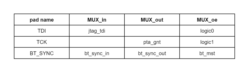
Let’s explain one pad example from given IO table with 3 different options – input, output, and inout:
-For the TDI pad, output-enable signal is 0, so the pad is configured as an input on the jtag_tdi line.-For the TCK pad, the output-enable signal is 1, so the pad is configured as an output which is driven internally, and can be seen on the pta_gnt line.
Given that the BT_SYNC pad has multiple functions, depending on the bt_mst signal, it’s behavior varies based on the configuration of the MUX. If the MUX is configured in a specific way, the pad will operate accordingly:
- when the mux output enable is set to 1, the pad acts as an output, driven by BT modul and equals to the bt_sync_out line.
- with mux_oe is set to 0, the BT_SYNC pad acts as an input, with an external source driving the pad. The value is then received on the bt_sync_in line.